


Çfarë është Dizajni i PCB-ve?
PCB (Printed Circuit Board) ose pllakë qarku të stampuar është procesi i dizajnimit të një platforme fizike për montimin dhe lidhjen e komponentëve elektronikë në një mënyrë të strukturuar dhe funksionale. Një PCB shërben si shtylla kurrizore e shumicës së pajisjeve elektronike, duke ofruar mbështetje elektrike dhe mekanike për komponentët që përbëjnë pajisjen.
Procesi i dizajnit përfshin krijimin e rrugëve të kalimit të rrymës (traces) që lidhin komponentë të ndryshëm si rezistorë, kondensatorë, IC (Integrated Circuits) dhe transistorë. Gjithashtu përfshin hartimin e një plani të pllakës që përfshin madhësinë, formën dhe llojin e komponentëve, si dhe rrugëtimin e lidhjeve elektrike.
Dizajni i PCB-së është një fazë kyçe në zhvillimin e produkteve elektronike, pasi përcakton jo vetëm funksionalitetin e qarkut, por edhe faktorë si besueshmëria, prodhueshmëria dhe kosto-efektiviteti.
Llojet e PCB-ve
PCB-të mund të ndryshojnë shumë në varësi të kompleksitetit, përdorimit dhe metodave të prodhimit. Më poshtë janë llojet kryesore:
1. PCB me Një Shtresë (Single-Sided PCB)
- Përshkrim: Komponentët montohen vetëm në njërën anë të pllakës, ndërsa ana tjetër përdoret për rrugëtim të traces.
- Aplikime: Kalkulatorë, lodra, sistemet e thjeshta të ndriçimit.
- Avantazhe: Kosto e ulët, e lehtë për prodhim dhe dizajn, e përshtatshme për qarqe me densitet të ulët.
- Disavantazhe: Kompleksitet dhe funksionalitet të kufizuar, mbështetje për numër të kufizuar komponentësh.
2. PCB me Dy Shtresa (Double-Sided PCB)
- Përshkrim: Ka traces elektrike në të dy anët e pllakës, të lidhura me vias (vrima të vogla).
- Aplikime: Burime energjie, sisteme kontrolli industrial, disa pajisje elektronike konsumatori.
- Avantazhe: Më kompakte se një shtresë, lejon më shumë komponentë dhe qarqe komplekse.
- Disavantazhe: Pak më e shtrenjtë dhe komplekse për prodhim, sfida në rrugëtim dhe vendosjen e komponentëve.
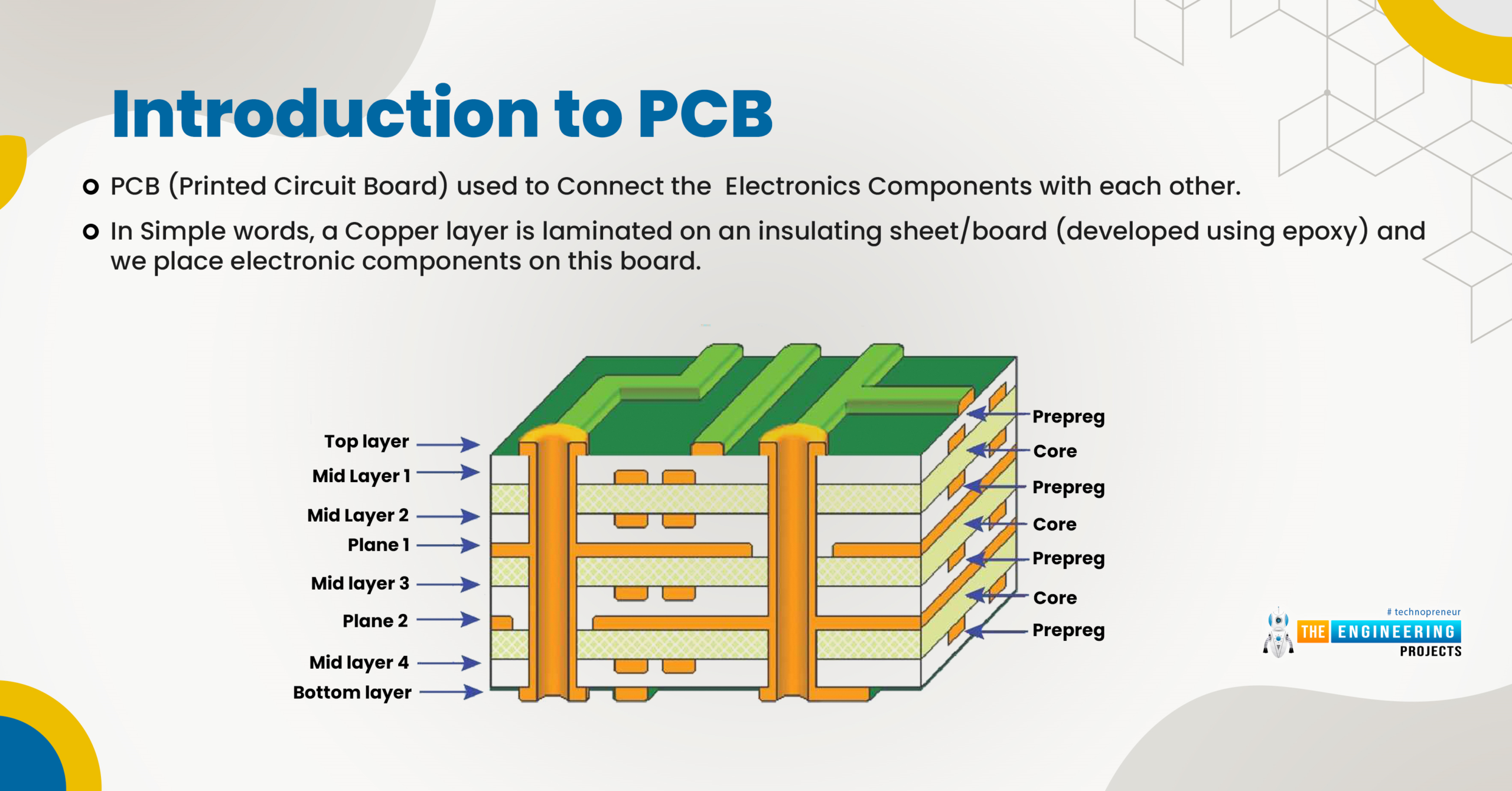
3. PCB Multi-Shtresë (Multi-Layer PCB)
- Përshkrim: Përmban më shumë se dy shtresa materiali conductor, të vendosura mes shtresave izoluese (4 deri 20+ shtresa).
- Aplikime: Smartphones, motherboarda kompjuterësh, pajisje mjekësore, telekomunikacion, automobila.
- Avantazhe: Densitet i lartë i komponentëve, dizajn kompakt, performancë elektrike më e mirë.
- Disavantazhe: Prodhim i shtrenjtë dhe kompleks, i vështirë për modifikim pas dizajnit.
4. PCB i Flexueshëm (Flexible PCB)
- Përshkrim: Bërë nga materiale fleksibël si polyimide, mund të paloset dhe të përkulet. Mund të jetë një, dy ose multi-shtresë.
- Aplikime: Pajisje të veshshme, ekrane fleksibël, pajisje mjekësore, elektronikë konsumatori.
- Avantazhe: Fleksibël dhe i lehtë, ideal për hapësira të vogla dhe lëvizje.
- Disavantazhe: Prodhim më i shtrenjtë, jetëgjatësi e kufizuar nën përkulje të vazhdueshme.
5. Rigid-Flex PCB
- Përshkrim: Hibrid midis PCB-ve të forta dhe fleksibël, me seksione rigide dhe fleksibël.
- Aplikime: Aeronautikë, ushtarak, pajisje mjekësore, elektronikë konsumatori me densitet të lartë.
- Avantazhe: Kombinon avantazhet e rigid dhe flex PCB, ideal për hapësira të vogla dhe aplikime të lehta.
- Disavantazhe: Shtrenjtë dhe kompleks për prodhim, kërkon teknologji të avancuar.
6. PCB me Frekuencë të Lartë (High-Frequency PCB)
- Përshkrim: Projektuar për sinjale mbi 1 GHz, përdor materiale speciale si PTFE ose qeramikë për të minimizuar humbjet e sinjalit.
- Aplikime: Telekomunikacion, radar, kompjuterë me shpejtësi të lartë, komunikim wireless.
- Avantazhe: Performancë e shkëlqyer në sinjale me frekuencë të lartë.
- Disavantazhe: Materiale dhe prodhim i shtrenjtë, dizajn kompleks.
Elementët Kryesorë të Dizajnit të PCB-ve
- Dizajni Schemati – Hartimi i diagrameve të qarkut me të gjitha komponentët dhe lidhjet.
- PCB Layout – Vendosja fizike e komponentëve dhe rrugëtimi i traces.
- Integriteti i Sinjalit dhe Energjisë – Siguron sinjale të pastra dhe energji të qëndrueshme për komponentët.
- Vendosja e Komponentëve – Minimizon gjatësinë e traces, shmang interferencat dhe optimizon menaxhimin termik.
- Rrugëtimi i Traces – Lidh komponentët sipas kapacitetit të rrymës, voltazhit dhe aftësive të prodhimit.
- Menaxhimi Termik – Përdor disipatorë, vias termike dhe plane bakri për të shpërndarë nxehtësinë.
- Design Rule Check (DRC) – Kontroll automatik për të siguruar që dizajni përputhet me kufizimet e prodhimit.
Aplikimet e PCB-ve
- Elektronikë Konsumatori: Smartphones, tablets, laptops, pajisje të veshshme.
- Elektronikë Automobilistike: ECU, sisteme infotainment, GPS, airbags, ABS.
- Telekomunikacion: Routera, switch-e, bazë stacione, pajisje celulare.
- Pajisje Mjekësore: Pacemaker, MRI, pajisje diagnostikuese.
- Elektronikë Industriale: PLC, furnizues energjie, robotikë, automatizim.
- Aeronautikë dhe Ushtarake: Avionikë, komunikim satelitor, radar, sisteme udhëheqëse raketash.
- Kompjuterë dhe Networking: Motherboard, karta grafike, switch-e rrjeti, servera.
Dizajni i PCB-ve është thelbësor për krijimin e pajisjeve elektronike moderne. Njohja e llojeve të PCB-ve, konsideratave kryesore të dizajnit dhe aplikimeve të tyre të ndryshme është e domosdoshme për inxhinierët, teknikët dhe dizajnerët elektronikë. Me avancimin e teknologjisë, kërkesa për PCB më të sofistikuara dhe me performancë të lartë rritet, duke nxitur inovacione në teknikat e dizajnit, materialet dhe proceset e prodhimit.
Nëse do, mund të bëj edhe një tabelë krahasuese të të gjitha llojeve të PCB-ve me avantazhet, disavantazhet dhe aplikimet për ta pasur gjithçka më të qartë dhe të shpejtë për referencë. Dëshiron ta bëj këtë?


